← Arduino Nano Schematics: Build Your Own Projects with This Guide Arduino nano pinout diagram pdf arduino nano pinout schematics images Push Pull Amplifier Schematic: High-Performance Audio Made Easy! 6l6 push pull amplifier schematics →
If you are looking for Slides developed in part by Prof. Dutta & Dreslinski - ppt download you've visit to the right web. We have 24 Images about Slides developed in part by Prof. Dutta & Dreslinski - ppt download like Component Placement in PCB Design & Assembly | Sierra Circuits, Mastering PCB Design Rules: A Comprehensive Guide for Optimal Results and also Component Placement in PCB Design & Assembly | Sierra Circuits. Read more:
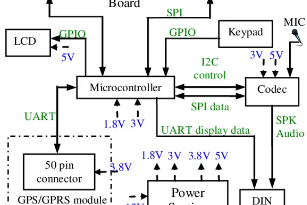
Slides Developed In Part By Prof. Dutta & Dreslinski - Ppt Download
 slideplayer.com
Slides developed in part by Prof. Dutta & Dreslinski - ppt download
What Are The Basic Steps Of Pcb Design - Design Talk
 design.udlvirtual.edu.pe
What Are The Basic Steps Of Pcb Design - Design Talk
Beginners Guide To PCB Routing: Tips & Best Practices
 circuits-diy.com
Beginners Guide To PCB Routing: Tips & Best Practices
Circuit Board Design
 ar.inspiredpencil.com
Circuit Board Design
High Speed Pcb Design And Layout, Expert PCB Design Service [ With Step
 www.venture-mfg.com
High Speed Pcb Design and Layout, Expert PCB Design Service [ With Step ...
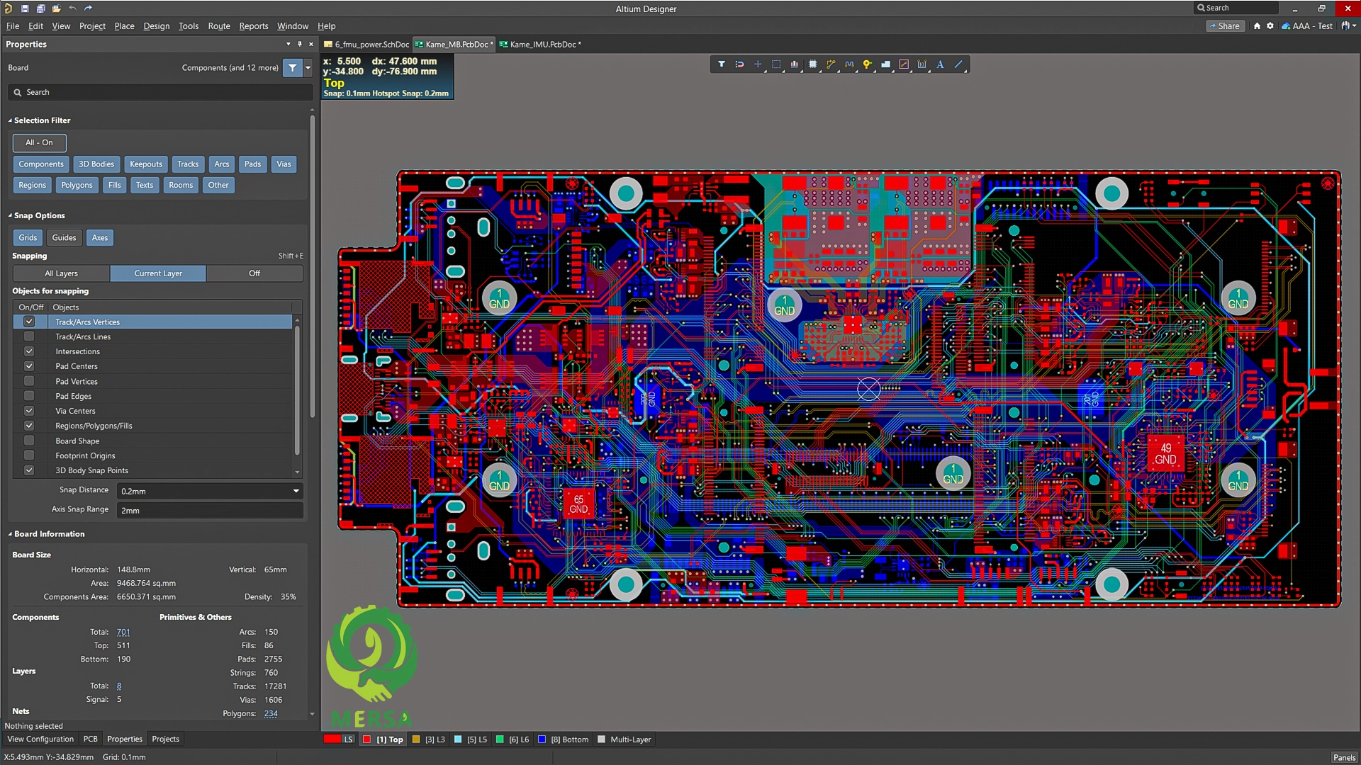
Double Layer PCB In Altium Designer Part-3: Layout Designing - YouTube
 www.youtube.com
Double Layer PCB in Altium Designer Part-3: Layout Designing - YouTube
Component Placement In PCB Design & Assembly | Sierra Circuits
 www.protoexpress.com
Component Placement in PCB Design & Assembly | Sierra Circuits
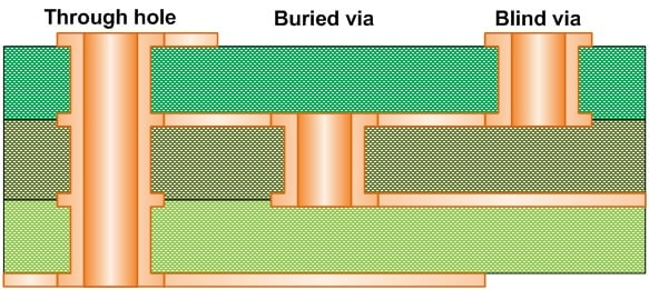
How And Where Use Vias In PCB Design
 www.proto-electronics.com
How and where use vias in PCB design
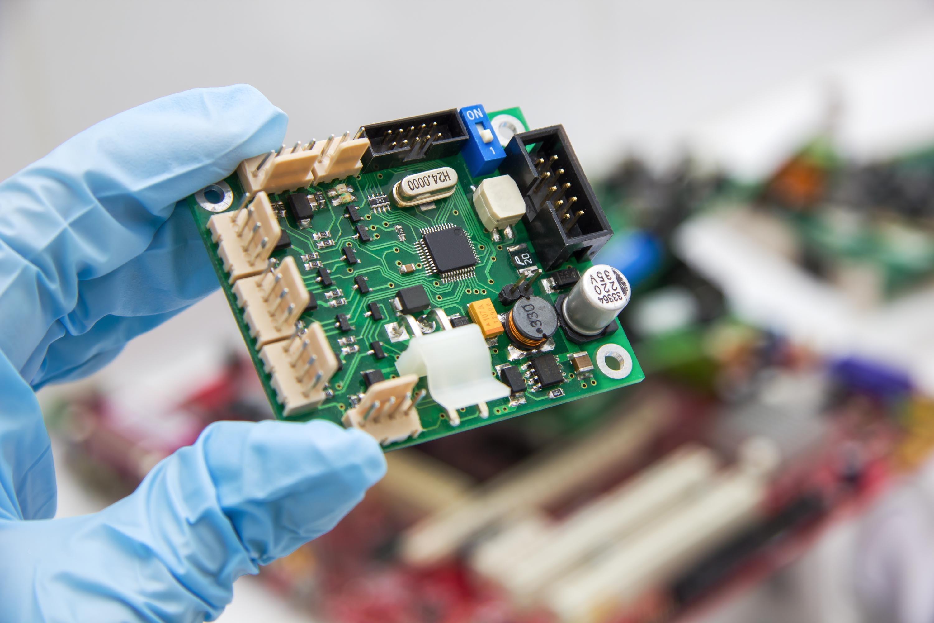
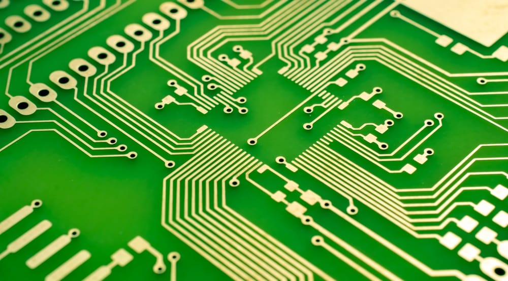
Basics Of A Circuit Board
 schematiclechfaniq.z4.web.core.windows.net
Basics Of A Circuit Board
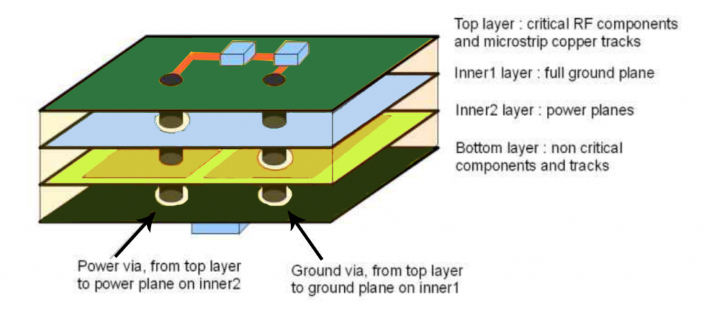
Tips About PCB Design: Part 3 - Static And Dynamic PCB Effects
 www.embedded.com
Tips about PCB design: Part 3 - Static and dynamic PCB effects ...
I-Connect007 Launches The Printed Circuit Designer’s Guide To…Secrets
 iconnect007.com
I-Connect007 Launches The Printed Circuit Designer’s Guide to…Secrets ...
CP2102 USB To UART Module PCB Design Project
 resources.altium.com
CP2102 USB to UART Module PCB Design Project
Fusion 360 - CNC Milling Your PCB Design / Part 3 - YouTube
 www.youtube.com
Fusion 360 - CNC milling your PCB design / Part 3 - YouTube
PCB Trace: The Backbone Of Modern Circuit Design
 www.wevolver.com
PCB Trace: The Backbone of Modern Circuit Design
معرفی 13 نرم افزار طراحی Pcb (دانلود نرم افزار طراحی برد)
 mersaelec.com
معرفی 13 نرم افزار طراحی pcb (دانلود نرم افزار طراحی برد)
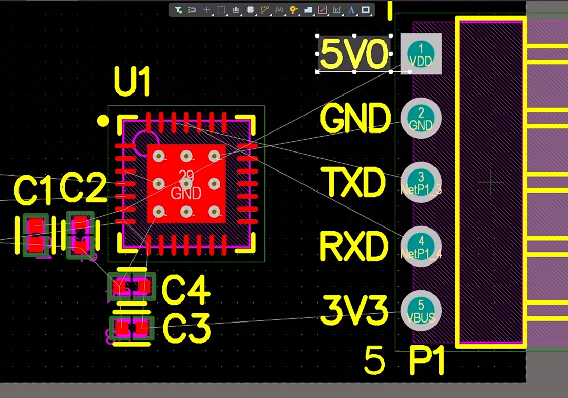
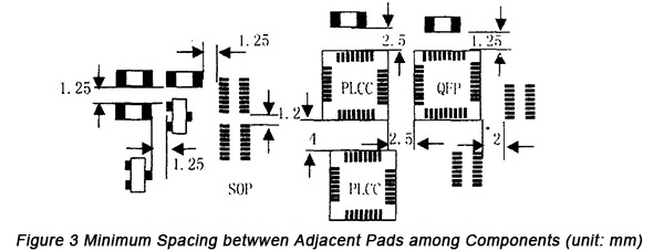
Design Requirement Of SMT PCBs Part Three: Component Layout Design
 www.pcbcart.com
Design Requirement of SMT PCBs Part Three: Component Layout Design ...
Cómo Diseñar Un Esquema De PCB: Una Guía Paso A Paso
 www.mokotechnology.com
Cómo diseñar un esquema de PCB: Una guía paso a paso
Basic PCB Design Rules That You Must Follow To Make Error Free PCB
 www.youtube.com
Basic PCB design rules that you must follow to make error free PCB ...
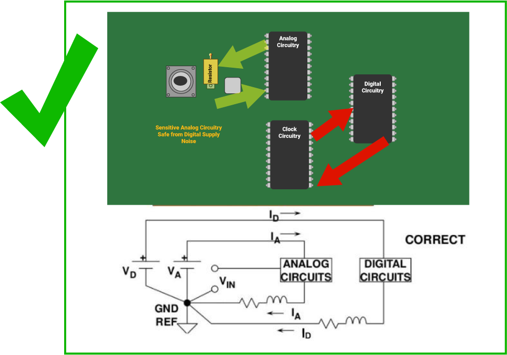
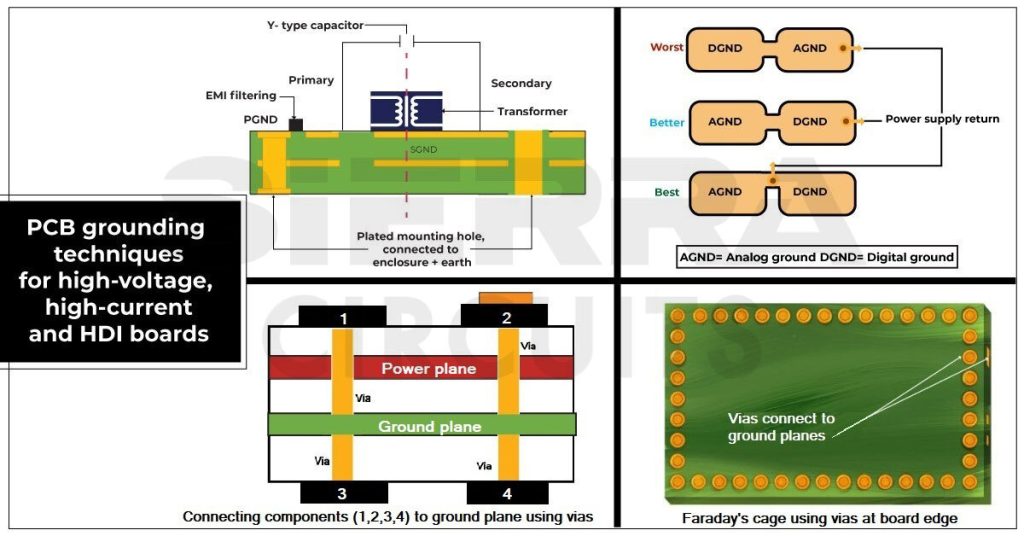
PCB Grounding Techniques For High-Power And HDI | Sierra Circuits
 www.protoexpress.com
PCB Grounding Techniques for High-Power and HDI | Sierra Circuits
Mastering PCB Design Rules: A Comprehensive Guide For Optimal Results
Mastering PCB Design Rules: A Comprehensive Guide for Optimal Results
How To Creat A GND For Your PCB Layout Design - Smt Assembly
 www.qhsmt.com
How to creat a GND for Your PCB Layout design - smt assembly
Component Placement In PCB Design & Assembly | Sierra Circuits
 www.protoexpress.com
Component Placement in PCB Design & Assembly | Sierra Circuits
An Ultimate Guide To Printed Circuit Board Design Steps And Basics
 hillmancurtis.com
An Ultimate Guide To Printed Circuit Board Design Steps And Basics ...
Understanding Proper PCB Design - Part 1 - Circuit Cellar
 circuitcellar.com
Understanding Proper PCB Design - Part 1 - Circuit Cellar
design requirement of smt pcbs part three: component layout design .... Circuit board design. How and where use vias in pcb design