← 2011 GMC Terrain Radio Wiring – Plug & Play! 2010 gmc acadia radio wiring diagram Photocell Wiring Diagram: Easy Installation Tips for Beginners 8 easy steps for photocell wiring: ultimate guide – moo wiring →
If you are looking for Designing a 4 Layer Stackup With 50 Ohm Impedance PCB Traces | Blog you've came to the right web. We have 25 Images about Designing a 4 Layer Stackup With 50 Ohm Impedance PCB Traces | Blog like Designing a 4 Layer Stackup With 50 Ohm Impedance PCB Traces | Blog, Designing a 4 Layer Stackup With 50 Ohm Impedance PCB Traces | Blog and also 4-Layer PCB Design Strategies - VSE. Read more:
Designing A 4 Layer Stackup With 50 Ohm Impedance PCB Traces | Blog
 resources.altium.com
Designing a 4 Layer Stackup With 50 Ohm Impedance PCB Traces | Blog ...
Designing A 4 Layer Stackup With 50 Ohm Impedance PCB Traces | Blog
 resources.altium.com
Designing a 4 Layer Stackup With 50 Ohm Impedance PCB Traces | Blog ...
Four Layer PCB Layout: Design Process And Cost Of Manufacturing
 hackaday.io
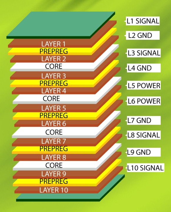
Four Layer PCB Layout: Design Process and Cost of Manufacturing ...
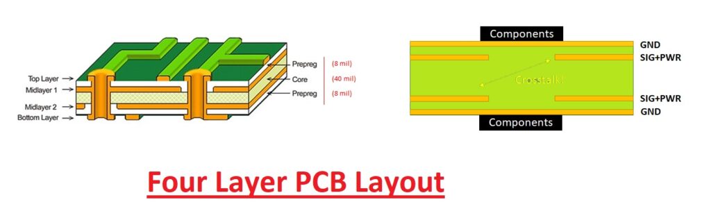
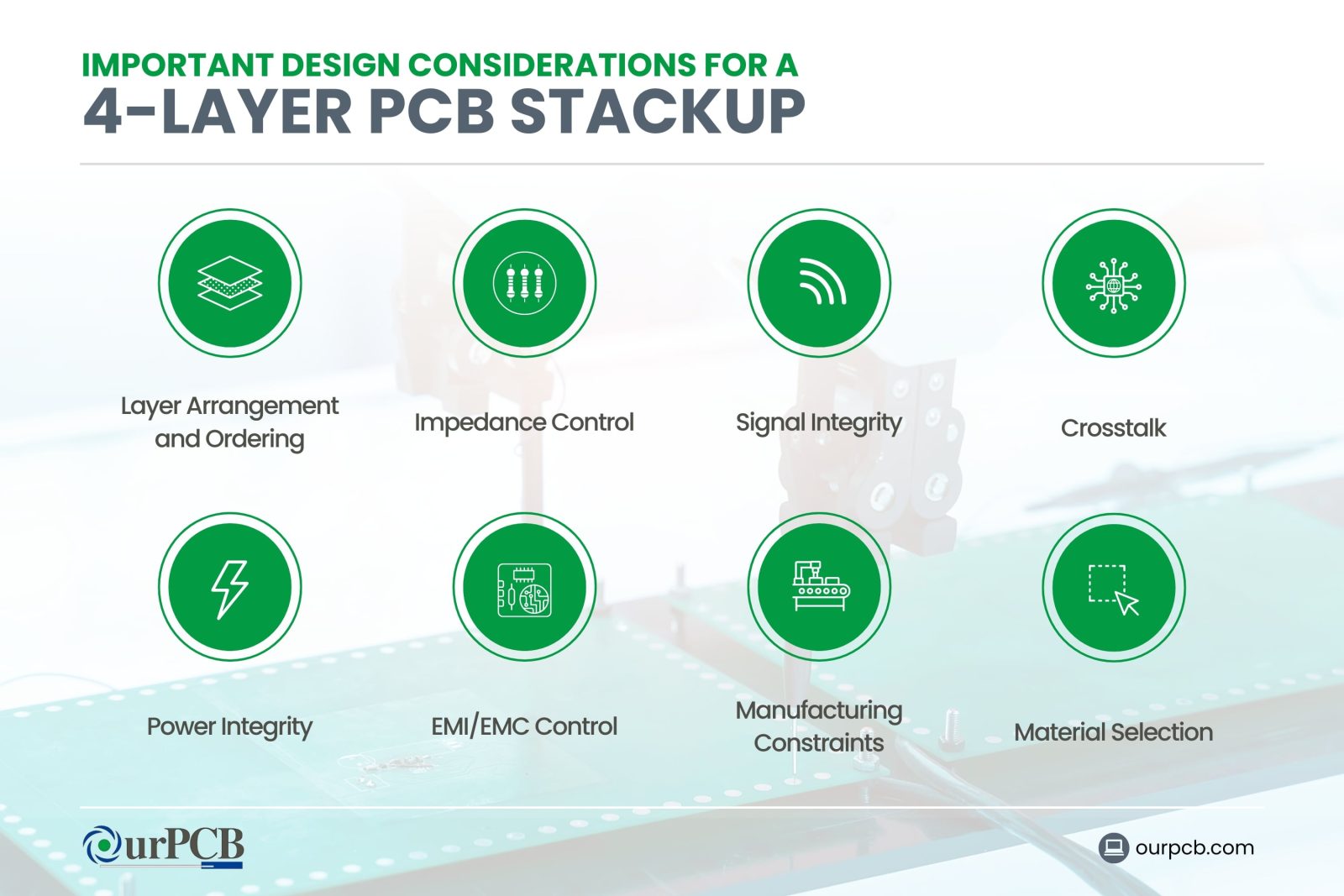
What Is A 4-Layer PCB Stackup? Examples & Guidelines
 www.ourpcb.com
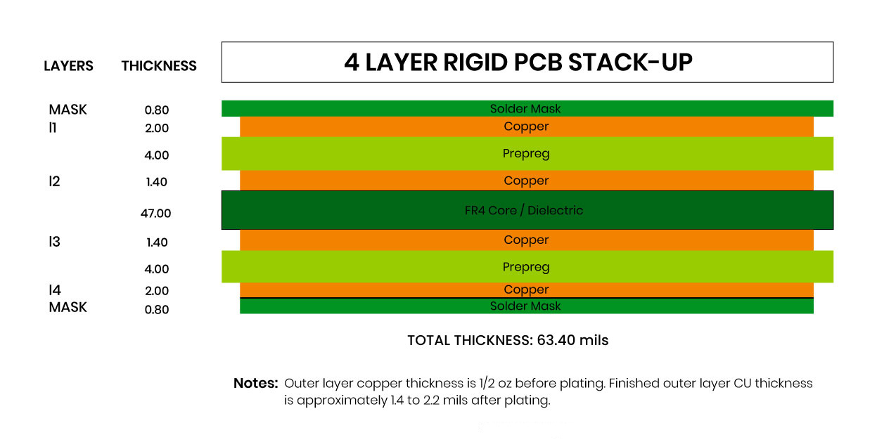
What is a 4-Layer PCB Stackup? Examples & Guidelines
Designing A 4 Layer Stackup With 50 Ohm Impedance PCB Traces | Blog
 resources.altium.com
Designing a 4 Layer Stackup With 50 Ohm Impedance PCB Traces | Blog ...
4-Layer PCB Design Strategies - VSE
 www.vse.com
4-Layer PCB Design Strategies - VSE
Design Of 50 Ohms RF Trace For 2.4GHz...Double Layer FR-4 PCB
 electronics.stackexchange.com
Design of 50 ohms RF trace for 2.4GHz...Double layer FR-4 PCB ...
An In-depth Analysis On PCB Stackup – PCB HERO
 www.pcb-hero.com
An in-depth analysis on PCB stackup – PCB HERO
Designing A 4 Layer PCB Stackup With 50 Ohm Impedance | Signal
 www.youtube.com
Designing a 4 Layer PCB Stackup With 50 Ohm Impedance | Signal ...
What Is A 4-Layer PCB Stackup? Examples & Guidelines
 www.ourpcb.com
What is a 4-Layer PCB Stackup? Examples & Guidelines
PCB Stackup And Trace Impedance Calculator In Altium Designer
 resources.altium.com
PCB Stackup and Trace Impedance Calculator in Altium Designer
Designing A 4 Layer Stackup With 50 Ohm Impedance PCB Traces | Blog
 resources.altium.com
Designing a 4 Layer Stackup With 50 Ohm Impedance PCB Traces | Blog ...
Designing A 4 Layer Stackup With 50 Ohm Impedance PCB Traces | Blog
 resources.altium.com
Designing a 4 Layer Stackup With 50 Ohm Impedance PCB Traces | Blog ...
Designing A 4 Layer Stackup With 50 Ohm Impedance PCB Traces | Blog
 resources.altium.com
Designing a 4 Layer Stackup With 50 Ohm Impedance PCB Traces | Blog ...
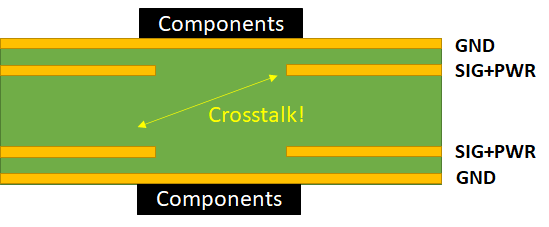
Two Alternative 4 Layer PCB Stackups With 50 Ohms Impedance | Blog
 resources.altium.com
Two Alternative 4 Layer PCB Stackups With 50 Ohms Impedance | Blog ...
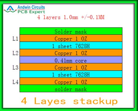
PCB Stack Up - Andwin Circuits
 www.andwinpcb.com
PCB stack up - Andwin Circuits
What Is PCB Layer Stackup?
 www.linkedin.com
What is PCB Layer Stackup?
PCB Stack-Up Guide & Examples | San Francisco Circuits
 www.sfcircuits.com
PCB Stack-Up Guide & Examples | San Francisco Circuits
Two 4-Layer PCB Stackups With 50 Ohms Impedance
 www.linkedin.com
Two 4-Layer PCB Stackups With 50 Ohms Impedance
PCB Stackup Design: Beginner's Guide | Reversepcb
 reversepcb.com
PCB Stackup Design: Beginner's Guide | Reversepcb
Designing A 4 Layer Stackup With 50 Ohm Impedance PCB Traces | Blog
 resources.altium.com
Designing a 4 Layer Stackup With 50 Ohm Impedance PCB Traces | Blog ...
PCB Stackup Guide: Optimizing Your Circuit Board Design
 hilelectronic.com
PCB Stackup Guide: Optimizing Your Circuit Board Design
4 Layer PCB Stackup - Engineering Technical - PCBway
 www.pcbway.com
4 Layer PCB Stackup - Engineering Technical - PCBway
PCB Copper Thickness & 4-Layer PCB Stackup In Panel Design
 sfxpcb.com
PCB Copper Thickness & 4-Layer PCB Stackup in Panel Design
Designing A 4 Layer Stackup With 50 Ohm Impedance PCB Traces | Blog
 resources.altium.com
Designing a 4 Layer Stackup With 50 Ohm Impedance PCB Traces | Blog ...
Designing a 4 layer pcb stackup with 50 ohm impedance. What is pcb layer stackup?. pcb stack up